Jose L. Agraz, PhD
para-Hydrogen Induced Polarization (PHIP)
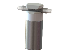
PHIP : Bo Current Control
Bo Stability Control
PHIP is a method applied to cell metabolites to enhance the MRI signal, allowing
for molecular imaging. The current flow generating a static magnetic field (Bo)
in a PHIP instrument has been discussed previously, but in most instances attention
has been directed towards the manual control of current flow using a voltage
controlled voltage source (VCVS) and feedback
from Hall sensors placed near the solenoid generating Bo.
The current flow produced by a VCVS often has inherent changes in
current stability, which is observed as noise. This noise often
changes rapidly such that manual corrections become insufficient, altering the Bo
and changing the nuclear resonance frequencies. In turn, this negatively affects
the maximum polarization achieved.
Voltage controlled current sources (VCCS), generally known as current sources,
are the foundation of electronic circuit design. They provide the basic current and
voltage conditions for electronic circuits to operate. Originally, current sources
were designed using resistors, however, due to size limitations, temperature instability,
and manufacturing variations, their use resulted in poor accuracy and
stability. In 1958, engineers at Crystalonics Inc developed the current regulator diode
(CRD), a small single component that produces constant current flow regardless of changes
in power supply voltage. Then, in 1964, Robert Wildlar developed precision current source
references which led to the μA702 design, the first commercial monolithic operational amplifier
(Op Amp). The development of quieter and more stable
current sources continues to this day, culminating with the development of the
high-stability, laser-trimmed, thin-film resistors, which allow for
current source designs with excellent initial accuracy, a very low temperature
coefficient, and an ultra-low noise level. These developments have been incorporated
in the design of one of today’s best voltage reference ICs, the Maxim MAX6126
(the device used in this VCCS design), a device with a wide operational temperature range,
ultra low noise & temperature compensation, high accuracy, and
force/sense outputs.
In addition to the theoretical and numerical simulations, we present comparative HEP
hyperpolarization results using a VCVS & VCCS. The models described
are based on transfer functions (TF), which supply the basis for finding the circuit
response characteristics without solving differential equations. First, we developed
the ideal VCVS & VCCS TF and impulse response to effectively demonstrating
the VCCS’ immunity to current flow fluctuations. Then, using Matlab we develop
the VCCS’ small signal model, which is estimated using the method of open
circuit time constants followed by the system’s output current/input voltage (VIin)
TF. Finally, we present the HEP hyperpolarization data showing a 50% better
polarization using the VCCS developed in our lab.
Ideal Voltage Controlled Sources Model Development
First, we consider the current flow impulse response of an ideal VCVS & VCCS powering a solenoid (L) in the s-Domain. Then, the resulting TFs show that a VCCS is a better choice than a VCVS for generating a Bo in PHIP applications. In circuit analysis and according to Watt’s law, an ideal VCVS maintains a given voltage difference between its terminals independent of the current drawn, while an ideal VCCS maintains a given current through its terminals independent of the voltage across its terminals. Any circuit can be modeled for analysis as a combination of voltage sources, current sources, and impedance elements. These models further simplify with the aid of Laplace transformations and TFs for circuit analysis in the s-Domain.
Ideal VCVS model
In order to obtain the VCVS circuit setup model as shown in figure 1a, we derive the resistor current (iT(t)) with a disruptive noise (impulse pulse) in the s-Domain using Kirchhoff’s law & the voltage diver rule in equation (1). Then, the VCVS circuit current impulse response is evaluated in the time-Domain (iR(t)), leading to equation (2), where L is the solenoid (40mH) and R is the current sensing resistor (1Ω). The resultant plot is displayed in figure 1b. The VCVS’ IR(s) change exponentially in the presence of a disrupting impulse pulse, making a VCVS design a poor choice for generating a stable Bo (fig 1).
Ideal VCCS model
Similar to the VCVS derivation, the ideal VCCS circuit setup model is shown in figure 2a. Using Kirchhoff’s law, the VCCS current flow is the same at any point in the circuit, as shown in equation (3), where k is a current flow constant (1 Ampere). The result plot is displayed in figure 2b. The VCCS’ current flow is a given constant, thus an ideal VCCS’ output current is immune to noise, making this design a good choice for generating a stable Bo (fig 2).
VCCS Model Development
We begin by describing the VCCS components: 1) An ultra high precision, ultra low noise, series voltage reference 2) A passive low pass filter, 3) An active low pass filter, 4) A MOSFET current sink and Op Amp with negative feedback, 5) Coil filter, and 6) Measure current port (fig 4 & 3). We employ various Matlab toolboxes to develop the VCCS small signal model, and consequent simulations result in the complete VCCS’ input/output TF (Io/Vin )
Voltage reference
The voltage reference used is a Maxim integrated ultra high precision, ultra low noise, series voltage reference. This reference has an ultra low noise to 1.3μVp-p from 1/10Hz to 10Hz, a ultra low drift of 3ppm/◦C with a ±0.02% initial accuracy
Passive Low Pass Filter
The passive low pass filter serves two purposes, the design uses a ten-turn potentiometer (R4) as a voltage divider to adjust I o and uses a low pass filter to minimize any electronic noise pickup through cabling (fig 5). As shown in equation (5), the complete filter’s TF has one zero (130K rad/sec) and two poles (-130K rad/sec & 307K rad/sec) (fig 5).
Active Low Pass Filter
The output voltage from the passive low filter is filtered by an active low pass filter, minimizing any residual noise (fig 5). As show in equation (6), this filter’s transfer function has two zeros (79x106K rad/sec, −0.2x10⁶K rad/sec) and three poles (31K rad, −11K rad, 12K rad).
Current Sink
The resulting output voltage from the active low pass filter drives the gate of a MOSFET setup as a current sink. In order to maintain control of the MOSFET drain current, an Op Amp is setup in a negative feedback configuration (fig 7). As shown in equation (7), the TF has three zeros (79x106K rad/sec, 0.2x10⁶K rad, 31K rad/sec) and four poles (3700K rad, -1800K rad, -3400K rad, -0.2x10⁶K rad). Notice that R9, C6, & R5 provide a filter to allow for most MOSFETs without changing the circuit, D5 provides protection for transients that may be produced by the main coil, C9, C11 lowers the resonance frequency of the main coil circuit, and R12 provides current drain and lower resonance frequency for the circuit.
Power Dissipation
Power dissipation at the current sink MOSFET is a key component to the circuit stability. As power dissipation increases because of increased current or/and power supply voltage, the current flow (Io) derates and is given by equation (8). For an optimal thermal noise level, the voltage drop across VDS must be kept at a minimum while keeping the MOSFET operating in saturation. If the VDS is too low, the power dissipation and thermal noise will be at a minimum, but may render the MOSFET useless. By trial and error, a VDS=1V yields the
Coil filter
As RF irradiates a given sample during molecular spin transfer, the RF sequence may induce a small magnetic field at Bo , causing a change in magnetic field, thus sample resonance frequency. Although, eliminating this effect completely is not feasible, by transforming the main coil into a tank circuit with a very low resonance frequency, the effect may be minimized. The resonance frequency for tank circuit is given by equation (3.9) and the bandwidth is given by equation (10). Since the tank circuit has a Fc =170 with a BW=400Hz, as long as the RF sequence frequency components are above 170+400/2=370Hz, noise induced into Bo will be minimum. Note that MOSFET capacitances are ignored, as the capacitances are in the nano Farads range, thus negligible at 370Hz (fig 9).
Measure current port filter
In order to keep track of the current flow through the main coil, a 1Ω current resistor was setup to allow voltage measurements, the current is measured indirectly using Ohm’s law (Fig. 10). Measuring the current accurately is a priority. Thus, a RC filter is setup for this purpose. The filter frequency is given by equation (11). However, the MOSFET’s resistance across the drain-source that forms the filter is dynamic by many factor such as; temperature, input voltage, power supply, and gate length (W). For a MOSFET working in the saturation region, the current through the MOSFET is given by equation (11), and solving for the resistance across the drain-source (ro ), ro is given by equation (13). Assuming all parameters in equation (13) except for VDS are constants, and VDS design target is 1v ±V noise , where V noise was measured at 150μV. Then, by Ohm’s law ro =1±150μΩ. Using equation (11) with R=r o and C=22.1μF, the filter frequency at the port is Fc =7.233KHz ±1Hz.
Temperature Sensor
In order to monitor temperature, our design monitors the ambient temperature near by through a precision temperature sensor LM35 with a full range given by equation (8). The output capacitance of the sensors is 50nF, a value too small to filter high frequencies at the output, thus, an additional capacitor was installed at C 22 =1μF
Current Flow Noise & Long Term Drift Experiment
We compare current flow noise (in) from a VCCS circuit designed in our laboratory and an off-the-shelf VCVS (Mastech HY3003D-3 power supply). The experiment demonstrates how a VCVS driving a solenoid results in poorly controlled current flow (Io), while a VCCS provides more stable Io and predictable Larmor frequencies over short and long periods. Bo and the Larmor frequency drift (F∆) for in and long term current drift (iD) are calculated using the BiotSavart law and the Larmor frequency equations. As shown in figure 12, we setup an experiment to collect current flow data as follows: 1) A solenoid is placed in series with a 1Ω 1% current sense resistor (R), 2) The current generated by the device under test (DUT) flows through the solenoid and the current flow indirectly measured using Ohm’s law [AK04], VR=Io × R. 3) V R is measured using an Agilent 34411A multimeter at the 1v range with a 1.5ppm resolution. Four sets of data were collected comparing the DUT’s in and iD. For each DUT’s in and iD, data was collected at 1.6KHz for 30 seconds and at 0.2Hz for 70 hrs respectively.
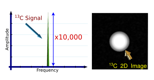
Hydroxyethyl Propionate Hyperpolarization Experiment
The PHIP hyperpolarization experiment setup for producing hyperpolarized hydroxyethyl propionate (HEP). The goal of the experiment was to produce hyperpolarized HEP using a VCVS and a VCCS for generating the Bo in a PHIP instrument developed in our laboratory. Then, the polarization obtained was compared for each DUT. The experiment performed for each DUT was as follows: 1) The DUT was installed in the PHIP instrument, 2) An HEA solution was prepared, 3) Each sample was run with the PHIP instrument’s polarization automated process, 4) Each HEP sample was collected and its polarization measured in a 9.4T Bruker Biospin Scanner.
PHIP Instrument Polarization Process
3mL of HEA solution was inserted into the PHIP instrument and the preprogrammed Labview automation software began the polarization process. In the PHIP process as seen in figure 13, the sample was heated for 45 seconds to 45C. While the sample was heated, the reaction chamber was filled with 99.8% para-Hydrogen gas at 4.8 bar. Next, the sample was pushed into the reaction chamber and the HEA hydrogenated to HEP with the catalyst’s aid. During the hydrogenation process, the sample was irradiated with a radio frequency (RF) sequence and the para-hydrogen spin order was transferred to the adjacent 13C nuclei. Finally, the sample was ejected out of the instrument and captured in a syringe.
Measuring HEP Polarization
The HEP sample polarization was measured with a 9.4T Bruker Biospin Scanner using a 90◦ hard pulse. The signal was acquired with a 20kHz spectral width at the 13C carbonyl resonance frequency.
VCCS Model
As shown in Table 2, the model (TF vccs) was solved for Io and evaluated at Vi
from 300mV to 1V, with two different loads, 1.5Ω & 4Ω. Then, the circuit’s Io
measured under the same loads. TF vccs (Io) data correlates with experimental data
to 0.02% at 0Hz. VCCS design is characterized by the TF’s dominant pole and
damping ratio. The dominant pole (ωd) determines the low pass filter prevalent
cut-off frequency and the damping ratio (ζ). ζ describes how quickly a disturbance
decays after being applied to our design. A ζ=1 means short decay, while ζ=-1
means a long decay. The design’s complete TF shows a ωd=49Hz & a ζ=0, failing
stability using the routh test with four negative real roots. The
passive low pass filter’s TF is shown in equation 5 with ωd =49Hz and a ζ=1.
The active low pass filter’s TF is shown in equation 3.6 with ωd =1.893KHz and a
ζ=1. The current sink’s TF is shown in equation 7 with ωd =296Hz and a ζ=-1.
A complete list of zeros & poles is shown in Table 1.
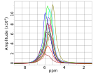
Finally, a total of 26 samples for VCVS & VCCS HEP polarization were
collected. For each sample, volume & peak area was recorded, and the peak area
was calibrated by volume. HEP polarization data is listed in Table 5 and plotted
in figure 16.
VCCS Model
 Introduction
 Software
 Bo Control
 Bo Noise
 Pinch Valves
 Conclusions
Feb 14th, 2015 at 5:09 pm